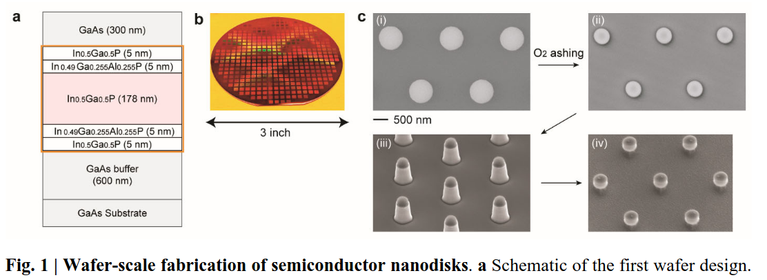
Photin grow wafers for scientists, who pursue goal of making the
smallest lasers: nanolasers disks also called laser nanoparticles.
We are nano-SME, supporting nanolasers development ;-).
The nano-size enable intriguing physical phenomena such as large Purcell
effects and threshold-less lasing, with mind blowing applications in
biological cellular
research,
and rapid microlab-on-chips (eg. flow cytometry of blood cells and
optical barcoding (marking) of single
cells.
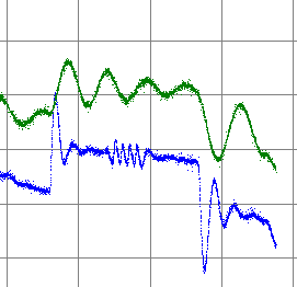
Our unique low temperature MOCVD technology with in-situ monitoring
allow us to see and control semiconductor layer properties with single
nanometer precision, like eg this unique view of in-situ reflectance
from strain-compensated MQW InGaAsP growth below.
The nanolasers active gain materials are III-V semiconductors such as
InP, InGaAsP and InGaP.
Supporting such fascinating research is pure joy for MOCVD engineers,
this is why Photin was founded, MOQ=1!
Enabling affordable science in area of III-V semiconductors!
Literature references:
- https://www.nature.com/articles/s41467-018-07248-0
- https://phys.org/news/2026-11-lasers-physical-limits-miniaturization-possibilities.html
- https://arxiv.org/pdf/2212.13301
- https://opg.optica.org/optica/fulltext.cfm?uri=optica-13-12-2415
- https://news.rice.edu/news/2026/rice-researchers-help-develop-lasers-near-physical-limits-miniaturization-opening-new