K. Kłos (Photin), C. Rivera (Waptel)
This post is the abstract submitted to the 11th Workshop on Semiconductor Lasers Physics and Technology, organized by Candela Foundation.
InGaAs/GaAsP superlattices (SLs) are actively developed worldwide, as the number of their applications increases steadily [1]. The main idea is to take advantage of the mature GaAs platform, and extend the wavelength of edge lasers, VCSELs [7], LEDs, SOAs, modulators, detectors [2], solar cells, and power converters from 870nm up to ~1050nm-1100nm, to match with the YDF fiber amplifiers ecosystem and technology.
Why InGaAs/GaAsP superlattices?
Mastering of InGaAs/GaAsP superlattices opens up high power, reliable Al-Free (ALFA) edge emitting lasers [3], which have enhanced lifetime/reliability, as they have higher thresholds for Catastrophic Optical Damage (COD) and for dark-line and dark-spot defects [4]. The same holds for VCSELs: the active region is Al-free, and indium slows down the growth of dark-line defects. In a same-structure comparison by Lumentum, where only the active region was swapped, 86 devices at 1060nm ran 5,000 hours at 115°C oven temperature with zero failures, while 850nm devices began wearing out within about 1,600-2,000 hours [7]. This kind of lasers is also suitable for implementing Buried Heterostructure designs, which require epitaxial regrowth [5]. Moreover, (Al,Ga,In)As-based structures cannot be epitaxially grown without undergoing relaxation, even at relatively low thicknesses.
Advantages of strain compensated InGaAs/GaAsP devices are well known to experts, and are subject to intensive research, such as DioHELIOS (Trumpf, ams-OSRAM, FBH, Jenoptik) to increase efficiency of high power lasers for nuclear fusion, or Al-Free lasers of Prof. Razeghi’s CQD in the US.
Why now: 1060nm VCSELs for AI scale-up
1060nm VCSELs, based on strained InGaAs quantum wells on GaAs, did not reach volume datacom in the years 2006-2015. The reasons were mainly market and infrastructure (850nm standards, installed fiber base, supply chain), rather than device physics [7]. The application has changed since then: AI scale-up links are greenfield, passive copper reaches just under 1m at 200G PAM4, while temperature and energy per bit became the dominant constraints. In 2026, Lumentum, Coherent, and Furukawa with FUJIFILM Business Innovation and Science Tokyo demonstrated 1060nm VCSEL arrays and transceivers for co-packaged optics [7].
The receiver and fiber side benefit as well: InGaAs photodiodes give 0.75 A/W at 1060nm, against 0.6 A/W for GaAs photodiodes at 850nm, and fiber attenuation is 0.95 dB/km against 2.09 dB/km [7].
The epitaxy is the demanding part. 1060nm emission needs about a third of indium in the wells, which is near the critical thickness limit, and requires GaAsP strain compensation. Without production volume, yield and cost of such structures stayed behind 850nm [7]. This is exactly the kind of structure described in this post.
It is fair to add, that the author of [7] expects coexistence rather than replacement: silicon photonics keeps the larger share of optical scale-up, while VCSELs get a real, but narrower niche of links from a few meters up to about 30m.
What was done
Photin studied the works of Hiromasa Fujii, who developed InGaAs/GaAs/GaAsP superlattice structures and provided many valuable insights about suitable setup and growth conditions [6]. Additional considerations were made regarding the accumulation of local elastic energy.
- HR-XRD profile of the grown SLs structure is shown in Fig. 1,
- PL map measurement of the wafer is shown in Fig. 2,
- MOCVD process development was supported with Filmetrics reflectometer, which allowed to observe epitaxial growth in-situ (Fig. 3), tune growth parameters, and see their effects in real time.
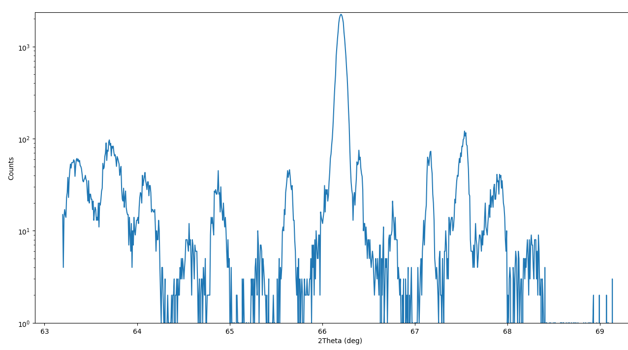
Fig. 1. HR-XRD characteristic of SLs structure
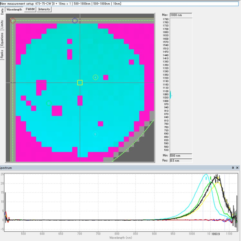
Fig. 2. PL measurement of SLs structure
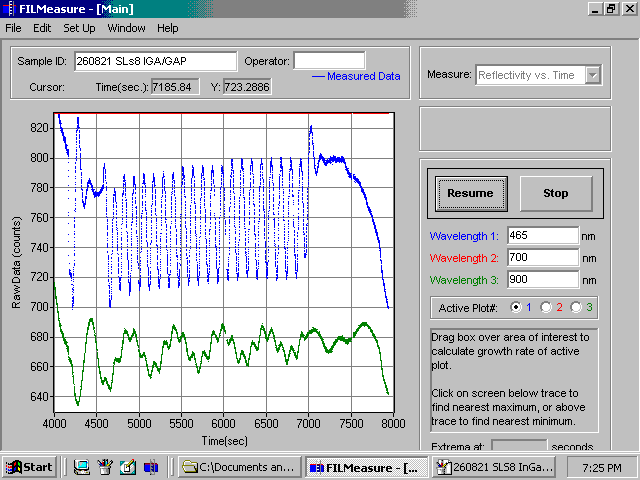
Fig. 3. In-situ reflectance trace from 465nm and 900nm wavelength
Available for researchers worldwide
This kind of structures can now be ordered from Photin at affordable price by researchers worldwide, in 2” wafer size. As far as we know, no other company or research institute in Poland demonstrated full PIN devices with technology of epitaxial growth of InGaAs/GaAsP superlattices so far.
Funding
This research is part of the DEMOGAAS (“Development and fabrication of basic building blocks for advanced modulators on a GaAs platform”) project, aiming to advance the development of an optoelectronic integrated circuit platform on GaAs, and has been partially funded by Spain Ministry of Industry and Tourism, under Order ITU/1144/2024, European Union Next Generation EU / PRTR.
References
[1] R. Tribout et al., “High‐Detectivity InGaAs/GaAsP Superlattice PIN Photodetector with a Thin Absorber on GaAs substrate for 1100 nm Applications,” Adv Elect Materials, vol. 12, no. 18, p. e70528, Sep. 2026, doi: 10.1002/aelm.70528.
[2] V. Letka et al., “InGaAs/GaAsP Superlattice Resonant Cavity-Enhanced Photodetector Fabricated on a Nominal Si(001) Substrate for Near- and Short-Wavelength Infrared Applications,” ACS Photonics, vol. 10, no. 9, pp. 3266–3274, Sep. 2023, doi: 10.1021/acsphotonics.3c00692.
[3] D. Botez, “Aluminum-free Technology Improves Diode Laser Performance.” [Online]. Available: https://www.photonicsonline.com/doc/aluminum-free-technology-improves-diode-laser-0001
[4] M. M. Apter and A. Salokatve, “Diode Lasers: New materials promise extended life.” [Online]. Available: https://www.laserfocusworld.com/lasers-sources/article/16555708/diode-lasers-new-materials-promise-extended-life
[5] R. Hogg, “III–V Epi advocates GaAs epi regrowth for emerging semiconductor laser applications.” [Online]. Available: https://www.semiconductor-today.com/news_items/2025/jan/iiivepi-270125.shtml
[6] F. Hiromasa, “Design, Growth, and Characterization of InGaAs/GaAsP Superlattice for High Efficiency Ge-based Multi-junction Solar Cells,” Mar. 24, 2015, University of Tokyo, doi: 10.15083/00008223.
[7] T. Li, “The Third Wave of VCSEL Demand: Why 1060 nm Is Back for AI Scale-Up,” Oct. 29, 2026. [Online]. Available: https://www.linkedin.com/pulse/third-wave-vcsel-demand-why-1060-nm-back-ai-scale-up-tao-li-w3zff/