Deep-tech physics inside Majorana 2 is topological superconductivity, and phenomena that occur between semiconductor-superconductor (indium arsenide antimonide-lead InAsSb-Pb). As epitaxy engineer, I skip in all high level details (protocols, measurements, Marjorana particles etc.). Will focus on core materials. What epitaxial layers form core stack of this approach to harness quantum physics in topological semiconductors realm? What is shown, and even more important, what is not shown, and get hidden? In company publications, this indicate, what is key challenge.
Majorana 1 (M1), earlier version relied on indium arsenide-alluminium (InAs-Al) interface. There is no detailed graph of first stack, but textual description in Supplementary information says:
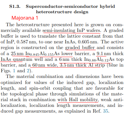
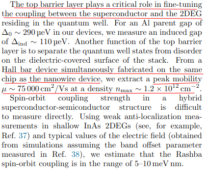
Informations about Majorana 1 semiconductor layers
It is interesting to note the Hall mobility obtained ~75k, which is really high. Hall sensors layers stacks with InAs QW reach ~35k. This type of M1 layer structure is similar to HEMT transistors on InP, where also mobility of thin In(Ga)As channel is maximized, and 2DEG of electrons in channel is induced by delta doping in barrier layer. It is very difficult to transition from InP to InAs with graded buffers, without getting dislocations, in so high number that they limit mobility of carriers.
Therefore, in Majorana 2(M2) Microsoft Quantum changed semiconductor portion of the device, using GaSb substrate (not semi-insulating!), and formed composite quantum well from InAs and InAsSb.
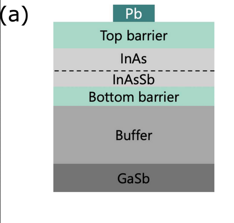
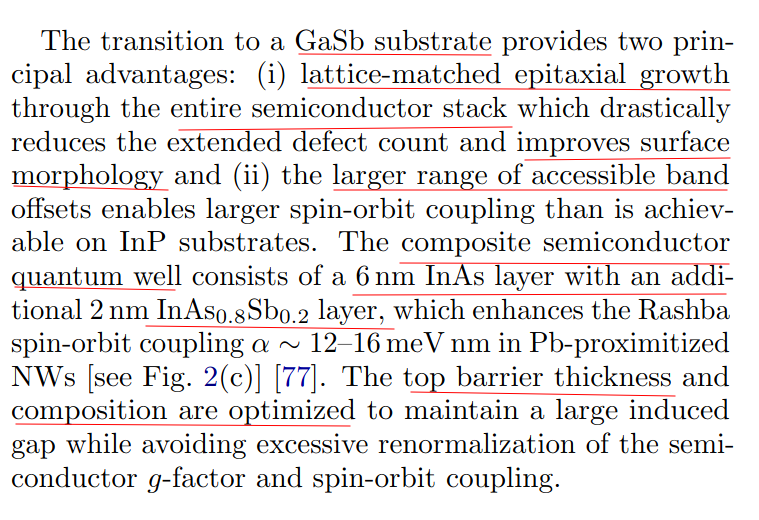
Informations about Majorana 2 semiconductor layers
Interestingly this time there is diagram of layers, but the compound used for barrier is not named. The TEM graph do not show almost any contrast between barrier and QW, which is weird. This device structure is somewhat similar in sequence of layers to ULTRARAM memory, which also has GaSb buffer, InAs channel, then InAs QW and AlSb barriers. In M2, to avoid dislocations, GaSb substrate was used, which has very low mismatch to InAs, and even better is fully lattice matched to InAsSb with ~10% of Sb. The MS wrote, that the full structure is lattice matched, but they not disclosed material barrier (btw. we know somehow M2 structure was grown by MBE ;-) ).
It is interesting to note that, it is barrier material, most critical
know-how.
The lattice matched barrier is the element, which is shared in core
quantum chips and MWIR-LWIR detectors and FPA arrays.
The barrier layers are explored with intensity in bleeding edge
research.
A few weeks ago QSIP 2026
conference
researchers from US, Korea UK and EU presented how they nurture the
growth and physics of barrier materials lattice matched to GaSb.
Search for (AlGaAsSb, barrier, InAsSbP). On the conference 4 compounds
were shown as solutions to make barriers on GaSb-based technology, and
growth of quaternary compounds are significantly more challenging than
binary InAs or ternary InAsSb:
- AlGaAsSb (standard in MBE by CEA Leti/CNRS, IAF, MUT, VIGO)
- InAsSbP (!Photin! by MOCVD)
- AlInAsSb (one US group)
- T2SLs with wider bandgap (Qiang Lee from Cardiff Univ.)
More info about materials: Magic of III-Vs
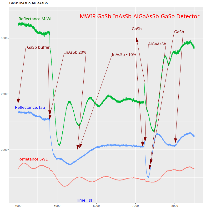
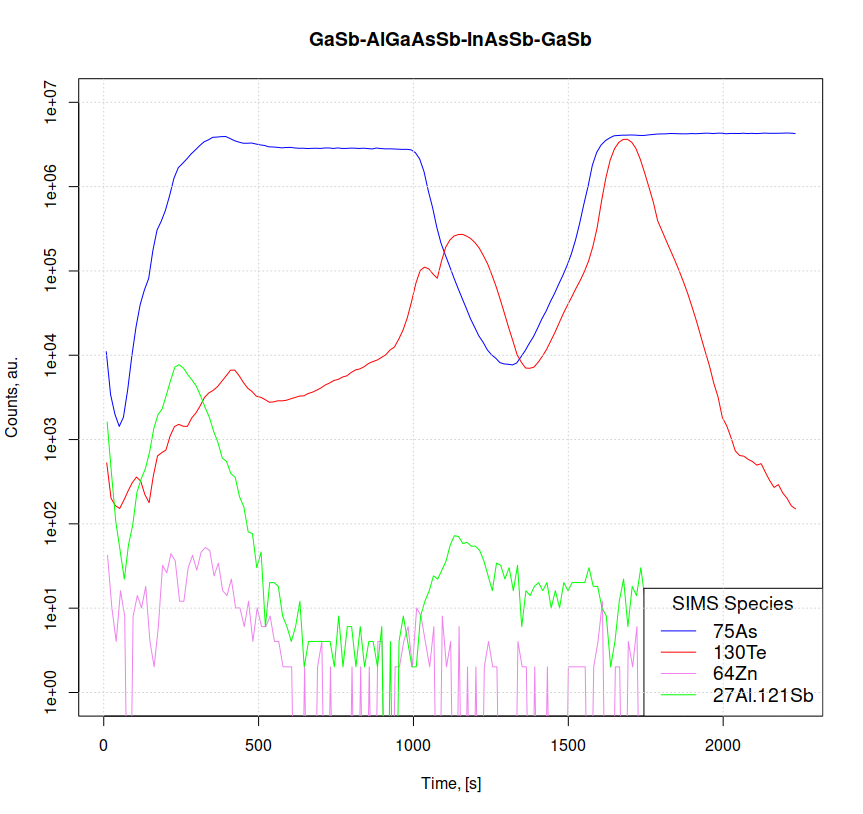
What is striking, is that Photin develop and grow similar structures very recently. Below is picture of In-Situ Refelectance and SIMS from growth of GaSb-InAsSb-AlGaAsSb-GaSb structure, which we use for MWIR Infrared Detectors development as final stages in InnoGlobo2 project.
In-situ reflectance and SIMS
In situ spectrometer monitor reflection from wafer as the layers grow. The blue curve shows short wavelength, where we could see how not lattice matched growth cause surface roughing (InAsSb 20%), correction of the Sb-flow (InAsSb 10%), which recover smooth surface, small peak from thin GaSb layer, and AlGaAsSb barrier layer being grown, with Zinc doping, and finally GaSb contact layer. Quick and rough SIMS profile shows that GaAs and InAsSb give similar level of As-signal, that Te-doped layer in end of GaSb buffer, Zn doping inside barrier and GaSb contact layer.
What is even more striking, is that state of the art InAs-InAsSbP
photodiode devices are being grown by MOCVD and LPE (not by MBE) using
InAsSbP barriers, which do not suffer from valence band offset and hole
barriers.
For now Photin+MUT+PWr photodiodes keep record for fastest single
barrier InAs photodiode: https://arxiv.org/abs/2605.26276.
The extraordinary speed of the InAs photodiodes is achieved due to high
mobility of carriers enabled by highest purity InAs absorber ~1e15cm-3
(full depletion of 1.45um at 0.8V) and lattice matched InAsSbP barrier
that do not impede mobility of hole transport.
GaSb-InAsSb is also used for research on topological insulators
Every new technology relies on background technologies developed before,
and Quantum is no exception.
It is very likely, that the core of QCPU of tomorrow, will be III-V
antimonide semiconductors, grown with epitaxial technologies developed
and refined for over 50 years before.
It is just another evidence, that Photin is developing key enabling
technology of the future, which will have countless applications in
devices of tomorrow.
#Made in Poland, #Made in EU
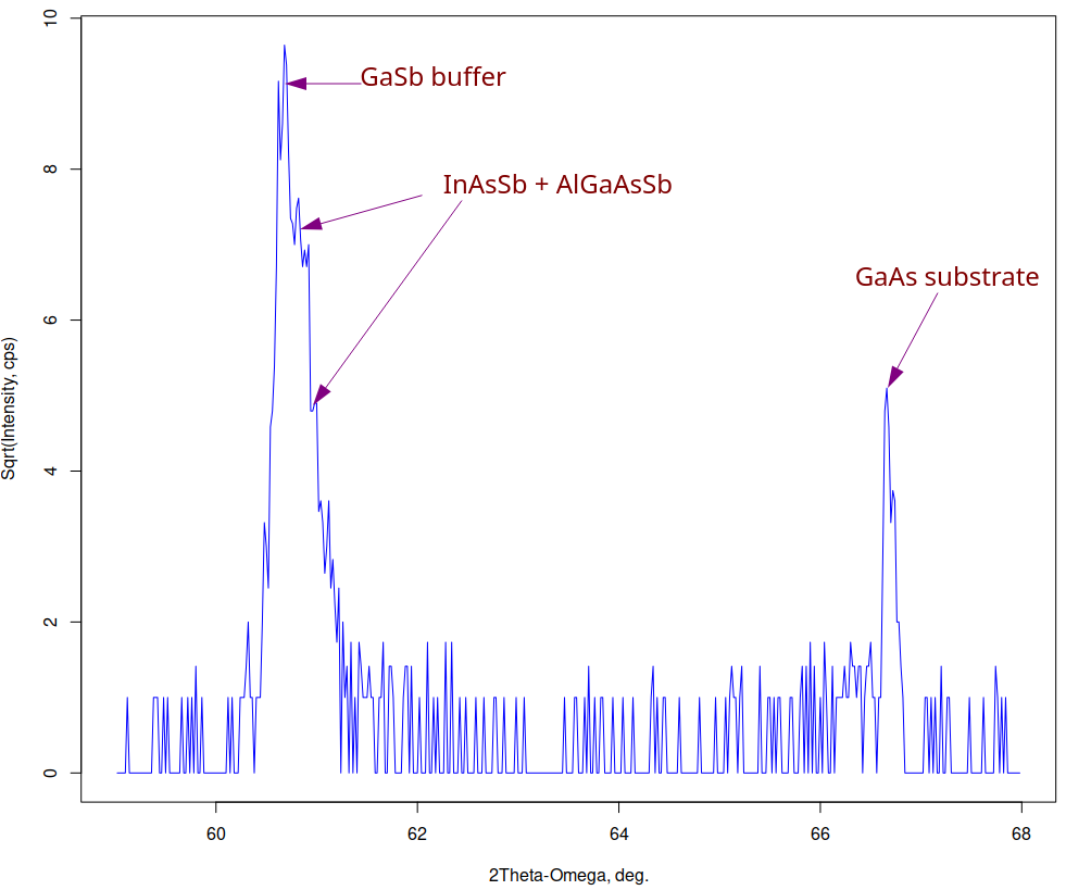
XRD of GaSb-InAsSb structure