They say: XX century = Electronics, XXI century = Photonics!
The success of GaN/SiC LEDs and Power, or InP-lasers and fiber internet
is our reality.
Have you ever thought, how the leap from Silicon to III-V compound
semiconductors (GaAs and InP) happened?
We hear so much about semiconductors in media. Not all semiconductors are alike, lets first make rough and debatable distinction:
- Silicon = electronics + detectors up to 1um wavelength + waveguides/fibers,
- III-V semiconductors = Photonics (emitters = LEDs, lasers, and detectors).
We take so many technology around us as natural, granted, mastered?
Without thinking how difficult were to advance the technology, how long
it took, who were the pioneer researchers developing it against
impossible odds. Millions watched and learned fabularized story of Shuji
Nakamura by Veritasium.
His personal crusade to get PhD for development of GaN-based LEDs and
lasers. Nakamura succeeded, “somewhat against” company he belong to:
Nichia, and obtained PhD! and Nobel prize. Nichia commercialized and
heavily benefited from Nakamura research.
(BTW. There are some diversion from real true story. eg. Nakamura not
build up his nitride GaN-AlGaN MOCVD, Nichia purchased commercial
reactor for him, and he modified it.
The picture of MOCVD reactor, shown in Veritasium movie is CCS TS from
Cambridge UK:
https://www.gan.msm.cam.ac.uk/facilities/reactors/thomas-swan).
There are also other pioneers and heroes worth to be recognized.
This post will be about other pioneer who worked on MOCVD technology of
III-V compound semiconduductors.
MOCVD = MOVPE technology is one of the most disruptive technologies
developed.
Thousands of MOCVD machines are working in Taiwan, another thousands are
in China. Most likely less than 100 machines are working in Europe. In
Poland, we could count “working” MOCVD machines on one hand, but Polish
government has Semiconductor Strategy
(https://www.gov.pl/attachment/dd1bd580-0106-4ce2-83e0-989ce574f773)!
We want to bring to wider community information about how, and who
started “low pressure MOCVD epitaxy revolution” of GaAs and InP based
materials. This materials are core of Lasers, Internet and Wireless
communication, sensing in SWIR revolution we experience around.
Spoiler, it is rather for engineers with some technical background.
Jean Paul Duchemin was the one of the very firsts (in team with
legendary prof. Razeghi from CQD), who worked on GaAs/AlGaAs and
InP/InGaAsP devices in Europe. After publishing his research results,
that sparked the revolution, he withdraw from the compound
semiconductors field and worked elsewhere for next 30 years.
He returned to epitaxy growers community in 2022, with one final
publication (https://doi.org/10.1016/j.jcrysgro.2022.126939) and
presentation, which he delivered at IC MOVPE XX conference in Munich.
It summarize his pioneering works, and could help technologist
understand better physics of III-V semiconductor growths, pitfalls, and
how the leap happened from Silicon epitaxy, to GaAs/AlGaAs and
InP/InGaAsP devices grown by low pressure MOCVD epitaxy.
The video cut out J.P. Duchemin final words. He appealed to Technology
Managers:
“Let the young generation of engineers experiment, make mistakes, and
search for new solutions!”.
In his speech he many times stressed, how his manager support enabled
this research.
Enjoy!
BTW. If you need 2” wafer based on GaAs, InAs, GaSb or InP, there is big chance Photin could grow it for you.

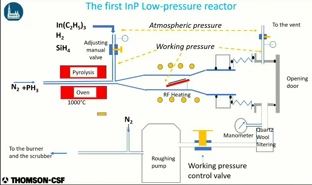
Early MOVPE reactor