Device results from Photin wafers
In 2024 our facility receive major upgrade with installation of Hydrogen
purifier based on Palladium Diffusion Membrane technology, which allow
to obtain ultimate purity of hydrogen for growth of semiconductors.
The performance of grown materials were tested on InAs on SI GaAs
substrates (to be reported soon) for wafer level characterization, and
InAs-InAsSbP structures for device results.
We arranged quick processing and measured a couple of 200, 300, 400 and
500um diameter photodiodes from InAs/InAsSbP structure to assess its
performance.
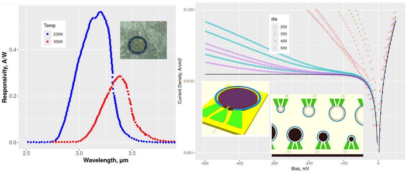
Small responsivity is justified, as this detector was illuminated
through InAs n-type substrate. Though, why dark current is so small?
Initially we thought that area normalization is wrong, or someone added
somewhere 100x factor by accident. The dark current looked too small,
and R0A too high..??
The 200-300 mesa size shows clearly larger dark currents due to sidewall
leakage currents. This highlight practical importance of research on IR
detector passivation, that is subject of our
InnoGlobo2
project with Military University of Technology.
Currently more samples from this wafer are being processed, to measure
it’s performance in illumination from top.
R0A as figure of merit of IR detectors
R0A product is a popular photon IR detector figure of merit. It is defined as the product of dynamic resistance at zero bias, R0A, by sensitive area, A. R0A is inversely proportional to the saturation current density Js of a photodiode:
R0A = kT / ( eJs)
It is possible to have high R0A, and low dark current, when the vallence barrier impede minority carrier transport and hence photocurrent, but this structure have reasonable responsivity @10mV despite being illuminated through InAs substrate. Additionally, for InAs-InAsSbP bandgap offsets are such, that they usually not form valence barrier, in opposite to InAs-AlAsSb or InAs-AlGaAsSb usually grown in MBE.
Investigation about InAs-based detectors performance
Hamamatsu, VIGO, Laser Components, Judson are the companies that offer InAs detectors, and their datasheets are first quick benchmark of what performance to expect.
| Vendor | Diam., um | R0Atyp, Ohm.cm2 | Rsh-min Ohm | Rsh-typ. Ohm | Jsat, A/cm2 | Datasheet |
|---|---|---|---|---|---|---|
| VIGO | 1000 | 0.51 | 50 | 65 | 0.051 |
 PVA-3-1x1
|
| Hamamatsu | 1000 | 0.55 | 40 | 70 | 0.047 |
P10090-01
|
| Judson | 250 | 0.15 | 200 | 300 | 0.180 |
J12-18C-R250U
|
| Judson | 1000 | 0.20 | 15 | 25 | 0.130 |
J12-18C-R01M
|
| Photin | 500 | 2.10 | NA | 1070 | 0.012 |
Ph-IA3.5-0.5-RT
|
| LaserComp. | 500 | 1.37 | 450 | 700 | 0.019 |
IA35
|
The R0A is in range of 0.2-0.55 Ohm.cm2, except for Laser
Components 1.37 Ohm.cm2.
Without doubt our results of 2.1 Ohm.cm2 clearly stand out.
Literature research at first sight shows a few publications, where InAs detectors were developed with parameters comparable to commercial :
- Janet Renee Pedrazzani PhD, MBE, Chap.5, R0A ~0.1 Ohm.cm2
- Benjamin White PhD, Sheffield Univ., MBE + MOCVD, 0.15 Ohm.cm2 or Jsat ~ 0.17 A/cm2 (at -0.5V),
- Zhou et al. Sheffield Univ. MOCVD, R0A ~0.1 A/cm2
Deeper search finally shown, that state of the art InAs detectors actually reach R0A ~2.0 Ohm.cm2, or equivalent 1e-2 A/cm2 dark current density, and it is not MBE InAs-AlAsSb, but InAs-InAsSbP materials:
- Chineese group using LPE technology,
- V.Tetyorkin et al. “InAs Infrared Photodiodes” report Ioffe devices reach 2.0 Ohm.cm2
Why it matters
III-V semiconductors are used for laser, detectors, modulators, SLEDs,
and Photonics Integrated Circuits. GaAs lattice matched compounds are
used for near infrared <1um, InP-based platform is used for 1um-~1.7um
range. InAs and GaSb based platform are used for SWIR, MWIR and LWIR
devices above 2um.
Looking at more mature InP-platform, we have 2 competing compounds,
AlInGaAs and InGaAsP. InGaAsP devices have poorer performance than
AlInGaAs, but lack of reliability risks without Alluminum, makes still
InGaAsP very popular compound for InP devices and PICs.
In InP-platform MBE technology use is limited for devices and PICs,
where multiple growths are required on single wafer, as MBE growth is
not conformal. Hence, majority of InP devices are grown by MOCVD, it is
technology of choice on market.
Type 2 superlattices InAs-InAsSb (T2SLs) are currently replacing HgCdTe
infrared detectors in commercial market of SWIR/MWIR/LWIR devices.
MBE technology in SWIR/MWIR/LWIR use InAs/GaSb or InAs/InAsSb T2SLs with
AlSb/AlAsSb/AlGaAsSb barriers. The Al-based barriers give reliability
risks in similar way to AlInGaAs in InP platform.
This is why we expect, that in longer term MOCVD InAs/InAsSbP will be
favoured for SWIR/MWIR/LWIR IR detectors and PICs applications.
Key take away
No other Polish company, institute or university was able so far to
showcase InAs ~3.5um detectors based on III-Sb semiconductors with
better dark current performance than our reported results.
Currently Photin ability to grow Sb-based, 6.1A family of III-V
compounds in MOCVD provide researchers unique opportunities in SWIR/MWIR
device development.