In recent 10 years, they are the one of the most researched material
concept for infrared (in particular solar cells and detectors). Aimed to
de-throne HgCdTe, material which still reign as the one with the best
properties for IR detectors, except …the manufacturability. Type II
Superlattices(T2SLs) made from InAs/InAsSb are actively developed in USA
JPL
NASA,
Israel,
China,
Poland included (VIGO + IMIF)! Though, like most of players in worldwide
(except UK), VIGO Photonics-MUT laboratory and Łukasiewicz IMIF use MBE
technology to grow InAs/InAsSb and InAs/GaSb Type 2 superlattices for
infrared detectors. MBE is usually selected for antimonides+arsenides,
though it is rather R&D technology, industrially more relevant is MOCVD
due to lower costs.
Photin decided to grow a few T2SLs structures, just to showcase
possibilities, and to test lines feeding MOCVD reactor with metalorganic
precursors (In, As and Sb), as T2SLs are also great technique to test
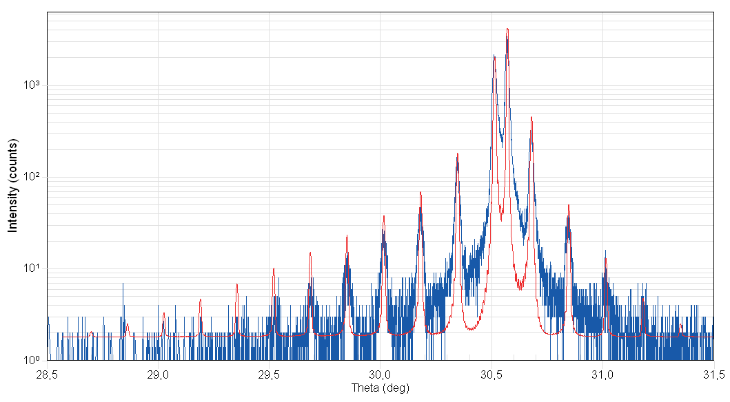
growth rates of InAs and InAsSb. To gauge T2SLs, single HR XRD
measurement is sufficient.
In future we might, continue this research topic, as separate project,
however it is clear landmark demonstration of our capabilities in area
of MOCVD technology. 12 years ago, PhD thesis of our CEO, lay foundation
for growth of HgCdTe detectors by VIGO/MUT laboratory. T2SLs are 3rd
generation materials of XXI century with multiude of applications, and
we were first in Poland to demonstrate MOCVD growth of InAs/InAsSb T2SLs
materials!
For now, we will continue ramping up and exploring the capabilities of
our MOCVD systems, tuning growth and doping of wide range of
antimonides, which are needed for InnoGlobo2 project and our customers.
Though no doubt, we will return to T2SLs sooner than later.