Semiconductors Technology Race
In XXI century, it is very rare and extremely difficult to develop
semiconductor device, which will beat commercial competition entrenched
on the market for half century. They had and have all resources:
Hamamatsu, Teledyne Judson, VIGO Photonics, etc. Hundreds and
thousands of man-years working on technology with customers, and
supported by state Universities.
We all see, that established semiconductor companies are heavily
subsidized by state, get hundreds of millions, and.. always ask for
more.
Though, it is not our case. Photin is startup, and all we have is
passion, and “Valley of Death!!
Lets celebrate, when true passion prevails!
It is magic moment, when after years of despair development on one of
the hardest deep-tech, customer ask:”Can you deliver more products like
this?”.
Independent Benchmark of Technology
When we presented in Feb 2025 our first chips-heroes results,
specialists were skeptical. “Yeess, Current-Voltage characteristics are
very good, but true responsivity is unknown, lets wait with celebrations
to see more relevant results”.
The first chips were illuminated from the substrate side, and reach only
~0.2A/W in 300K.
Three different labs!, each with 30+ years of experience in
processing technology, were given our samples.
Aim: process and test PD InAs wafer sample, to obtain feedback about
performance of our technology.
The tests were done on hundreds of chips, multiple processing
cycles.
And now, half year later, we could present comparison of Responsivity,
Rshunt, and YIELD, which confirm our technology performance.
Responsivity of InAs detectors
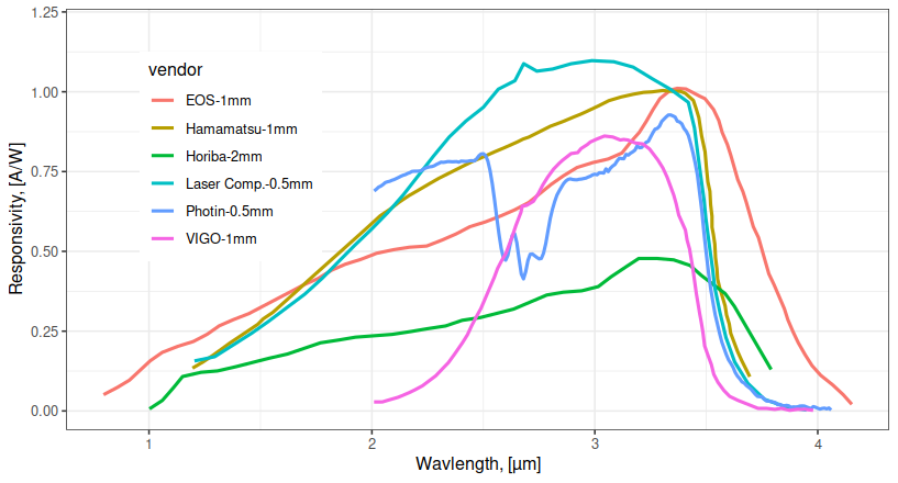
Comparison of responsivity on top illuminated InAs photodiodes.
Photin and Laser Components are 0.5mm dia devices (which could give ~10%
sensitivity increase). VIGO and Hamamatsu are 1mm dia, Judson put 0.25mm
dia responsivity to datasheet, which looks like generated with max 1.5A,
not measured for 22degC.
Photin InAs PD has the best responsivity below 2µm, and enhanced
sensitivity around 3.4µm, the dip around 2.7µm is moisture in air.
VIGO PD clearly is of selective type (optimized for H-C hydrocarbon
detection), and has relatively short cut-on around 2.5µm, and quite low
maximum responsivity.
Laser Components PDs has quite thick absorber, with high Rsh which give
them superior Ri in 2.2-3.4µm range.
“Cut-off” wavelength of VIGO PD is visibly shorter, than rest. This
looks like measurement at lower than room temperature, to increase Rsh
and get slight responsivity boost.
EOS looks like add some Sb, to extend cut-off to longer wavelengths.
Horiba 2mm dia chip clearly shows, how larger area reduce responsivity.
There are a few types of InAs photodiodes, which differ with responsivity:
- wide 1-3.5µm devices (front side illuminated),
- selective eg. 2.5-3.5µm (back side illuminated through layer which define cut-on eg. InAs, GaSb, or InAsSbP layer)
- filtered where window with band pass filter select part of responsivity spectrum.
Responsivity is function of absorber thickness, usually ~2-3µm layer to
get 0.8-1.1 A/W.
Thickness of absorber layer also affect capacitance and speed of
photodiode.
The true superiority of Photin InAs PD devices is manifested, when PDs
with larger optical area are made 1-2mm dia.
~4x smaller Rsh of VIGO, Judson and Hamamatsu InAs 300K photodiodes,
give chips with reduced sensitivity in centre.
Hence we could expect, that 2mm and 1mm PDs from Hamamatsu or Judson,
will actually not manifest of the full responsivity of 1.1-1.5 A/W max,
but much lower actually.
4x larger PD resistance should give ~20% better responsivity in the
centre of detector for Photin PDs, in comparison to competition.
![Mechanism of reduced sensitivity in PD centre due to small Rsh [Judson].](/../assets/img/250821_Photin-InAs-Passed-Qualifications/sensitivity_loss_on_large_areas.png)
Mechanism of reduced sensitivity in PD centre due to small Rsh \[Judson\].
![Mechanism of reduced sensitivity in PD centre due to small Rsh[Hamamatsu].](/../assets/img/250821_Photin-InAs-Passed-Qualifications/sensitivity_loss_on_large_areas_hama.png)
Mechanism of reduced sensitivity in PD centre due to small Rsh\[Hamamatsu\].
Shunt Resistance
Responsivity could vary 5-10%, and it is quite easy to increase it by thicker absorber, so it is not too big factor in PD detectivity (figure of merit). The true performance benchmark is still I-V curve, and Rsh of the devices (which could vary ~400%), and YIELD DISTRIBUTION!!
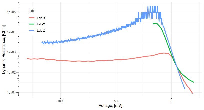
Comparison of best Rsh results from 3 labs
Even worst result of Lab-X is still ~600 Ohm Rsh for 500µm dia, equivalent of 150 Ohm at 1mm dia, which is still 3x better than Min. specs of Hamamatsu and VIGO, and 6x better than Typical specs of Judson InAs PDs.

VIGO Photonics DataSheet

Hamamatsu DataSheet

Teledyne Judson DataSheet
Comparing the specs we see, that the Western companies developed other
technology of InAs devices, based on InAs homo junctions by LPE or
InAs/AlAsSb by MBE.
Our devices are matching the specs of the technology developed in East
by Russian scientists from companies, which spin out of Ioffe (MIRDOG,
LMSNT), and most likely Laser Components, SciTec, Boston Electronics and
Roithner were their distributors. Also some China scientist shown
InAs/InAsSbP PD grown by LPE, with similar performance to Photin.

LSMNT 500um dia InAs PD DataSheet
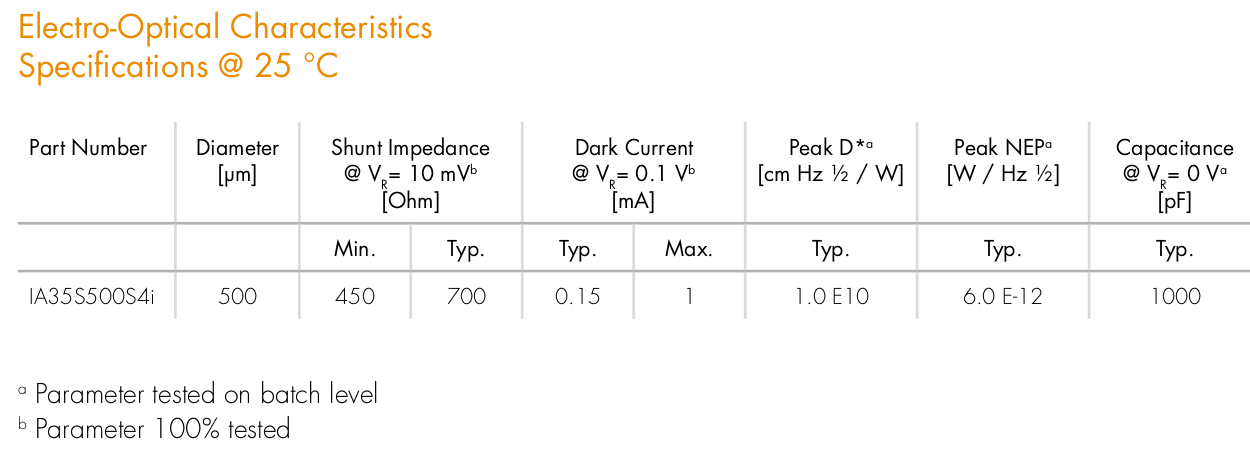
Laser Components 500um dia InAs PD DataSheet
LSMNT 0.5mm dia Min. specs of 200 Ohm is equivalent of VIGO 50 Ohm
(divide by 4), but Typical specs. value is much higher 2.5x more. Even
higher are specs of Laser Component with Min. 400 Ohm (100 Ohm 1mm dia
equivalent), and 700 Ohm Typical (150 Ohm 1mm dia equivalent).
Those are most likely the best chips, which are sold at highest price
for applications demanding highest performance. Still Photin could
provide also such state of the art chips, the only question is with what
YIELD?
Yield = Profitability
It is quite rare for semi companies to provide info about yield of their
technology and products. Very often yield is not constant, and vary
between processings campaigns.
Once on conference we have seen info about yield of Extended InGaAs
2.6µm PDs from VIGO Photonics.
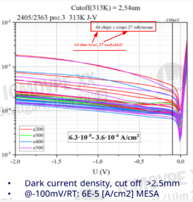
Dark Current statistics for 64 chips of 2.6µm extended-InGaAs PDs by VIGO.
We could see here, that 27 chips were so bad, it was not worth to show them. On the graph, we could see ~7 more poor chips (2x e500 pink which should be better, 4x red e200 have leakage, and 1x blue). So yield in this case was ~47% of good chips.
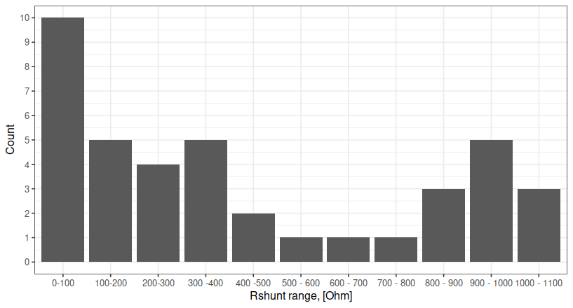
Yield on Photin InAs PD wafer sample with 40 chips
In the case of our InAs PD samples, yield is similar. If we impose Laser
Components specs, then yield is ~35%, which is not too bad for first
experiments. If we would set min Rshunt with VIGO, and Hamamatsu specs,
then 62.5% yield would be achieved. With specs from Judson 75% yield.
In any case this technology will be developed further, to increase yield
and provide customers state of the art devices.
It is still amazing to see that, 8x chips of 40, have Rshunt 300%
better, than Typical Western commercial company specs like VIGO,
Hamamatsu or Judson!!!
Key take away
Photin demonstrated state of the art performance of InAs PDs are
possible from wafers grown by our MOCVD, and get first PD product
qualified, with reasonable yield.
The demonstrated devices specs surpass renowned Western companies like
VIGO, Hamamatsu and Teledyne-Judson.
Good InAs/InAsSbP results are proof of concept, that MOCVD technology
could be extended to bulk GaSb/InAsSb, and InAs/InAsSb T2SLs devices,
which could reach out toward highly valued longer MWIR and LWIR
wavelengths.
In future InAs/InAsSbP could become platform for MWIR Photonics
Integrated Circuits, similarly as InP/InGaAsP is platform for
DataCom/Telecom Integrated Photonics in Near Infrared.