Have started GaSb buffer development with cleaving Ensemble3 GaSb Zn-doped substrate (bought from EVO-R funds) to 6 pieces, and running experiments.
In literature, not able to find info about the GaSb growth conditions with TMGa + TMSb, for Aix-200 type of reactor. There were a few excellent info, especially TEGa + TESb (which was also used by our partner FZU), and we used them as start point.
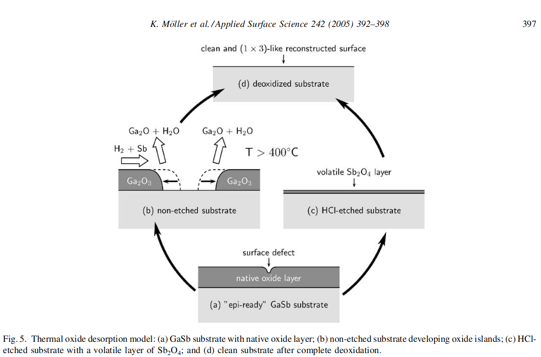
For preliminary parameter scan for GaSb optimization, decided to not etch substrates, so would get larger roughness and characteristic “oxide defects patterns”, but still the optimum V/III ratio should be clearly distinguishable.
")
") Fig. 2. Nomarsky picture of surface with “the hillock” type of defects.
Fig. 2. Nomarsky picture of surface with “the hillock” type of defects.
Around the run nr 4 the faith, that 1 substrate will be enough to
optimize GaSb-on-GaSb buffers begin to tremble ;-), and we have split
two the biggest pieces in half to get 8 pieces in total, and increase
odds.
Also first runs indicated that the TMGa Pressure Controller is not
stable, and cause molar flow spikes.
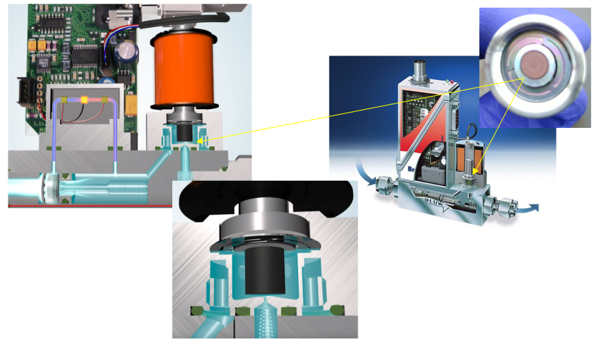
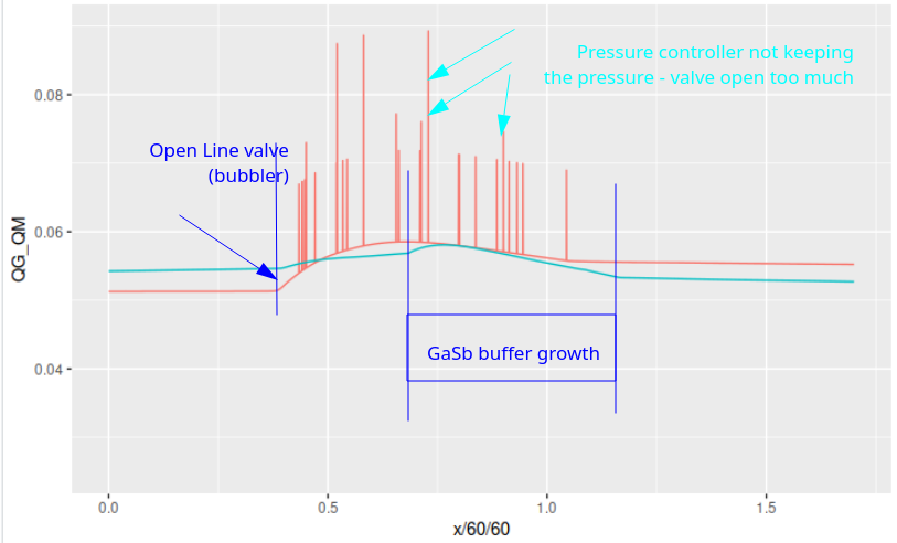 Fig. 3 Construction of MFC/PC(left) and graph of log Sb/Ga ratio
recorded by 2x ultrasonic precursor monitors.
Fig. 3 Construction of MFC/PC(left) and graph of log Sb/Ga ratio
recorded by 2x ultrasonic precursor monitors.
Photin have dozens of spare Pressure Controllers (PC), and 3rd
replacement worked ok, not showing spikes in graphs of molar flow. This
kind of spikes (caused by too large opening of valve), could cause
complete disaster especially, for ultrasonic monitors in closed-loop
control mode with PID control (Episons). Our ultrasonic monitors do not
have PID, so it would be less problems, but still it is better to have
PC working without issues. This kind of problems with PC, are difficult
to detect without ultrasonic monitors.
Eventually, narrowed down the optimum GaSb buffer parameters with one
substrate, in 8 runs, ~1 week.
 Fig. 3. Comparison of pictures taken by microscope with Nomarsky
contrast.
Fig. 3. Comparison of pictures taken by microscope with Nomarsky
contrast.
As could be seen, in run nr #5 set proper Sb / Ga ratio, then explored
going into a little Ga-rich buffers #7 and #8 to make sure, that
optimal Sb /Ga ratio was found. Pictures shows that run nr #5 had best
surface smoothness.
Key take away, is:
-
Te-rich GaSb give surface with hillocks patterns,
-
Ga-rich GaSb give streaky lines, that transition into Ga droplets on surface,
-
establishing proper Ga / Sb ratio for TMGa + TMSb in our reactor,
-
ability to keep and reproduce exactly optimum Ga / Sb ratio with help of ultrasonic monitoring devices.
Comparing side by side buffers grown by FZU (TEGa + TESb, substrate HCl etched before loading) with buffers grown by Photin (TMGa + TMSb, not etched substrates).
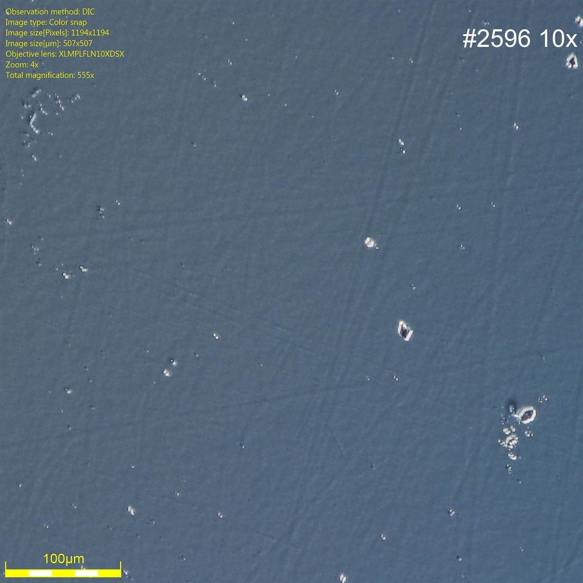
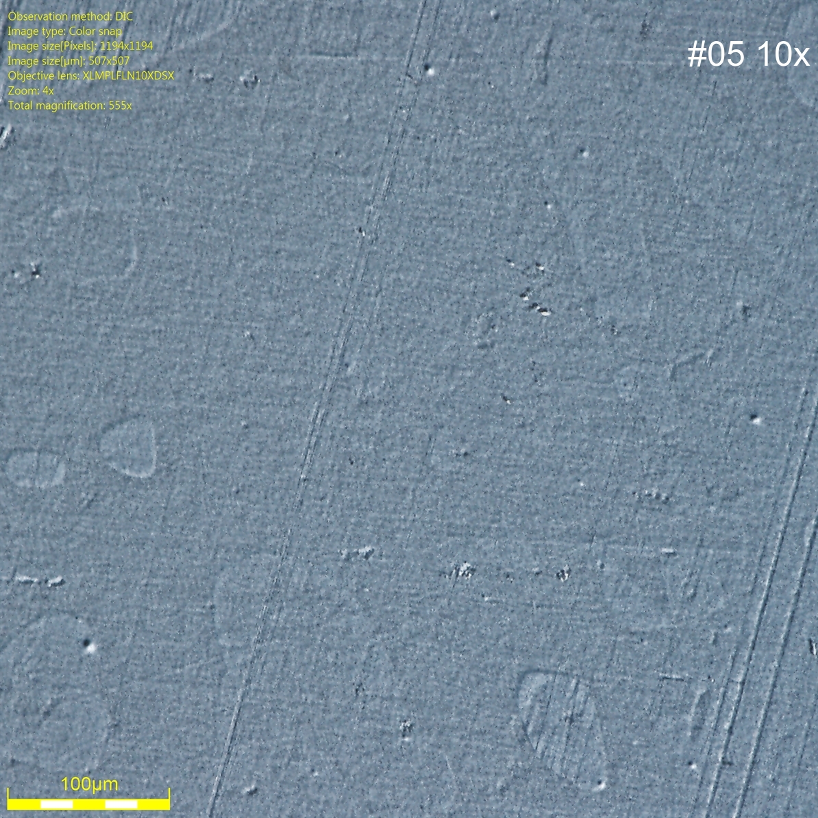
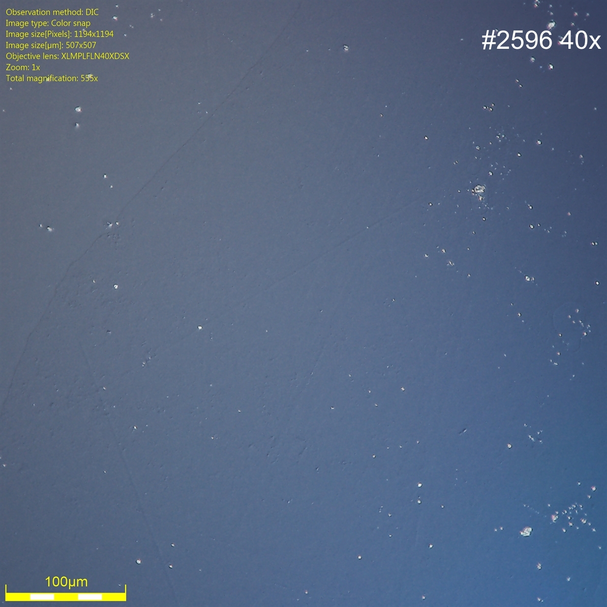
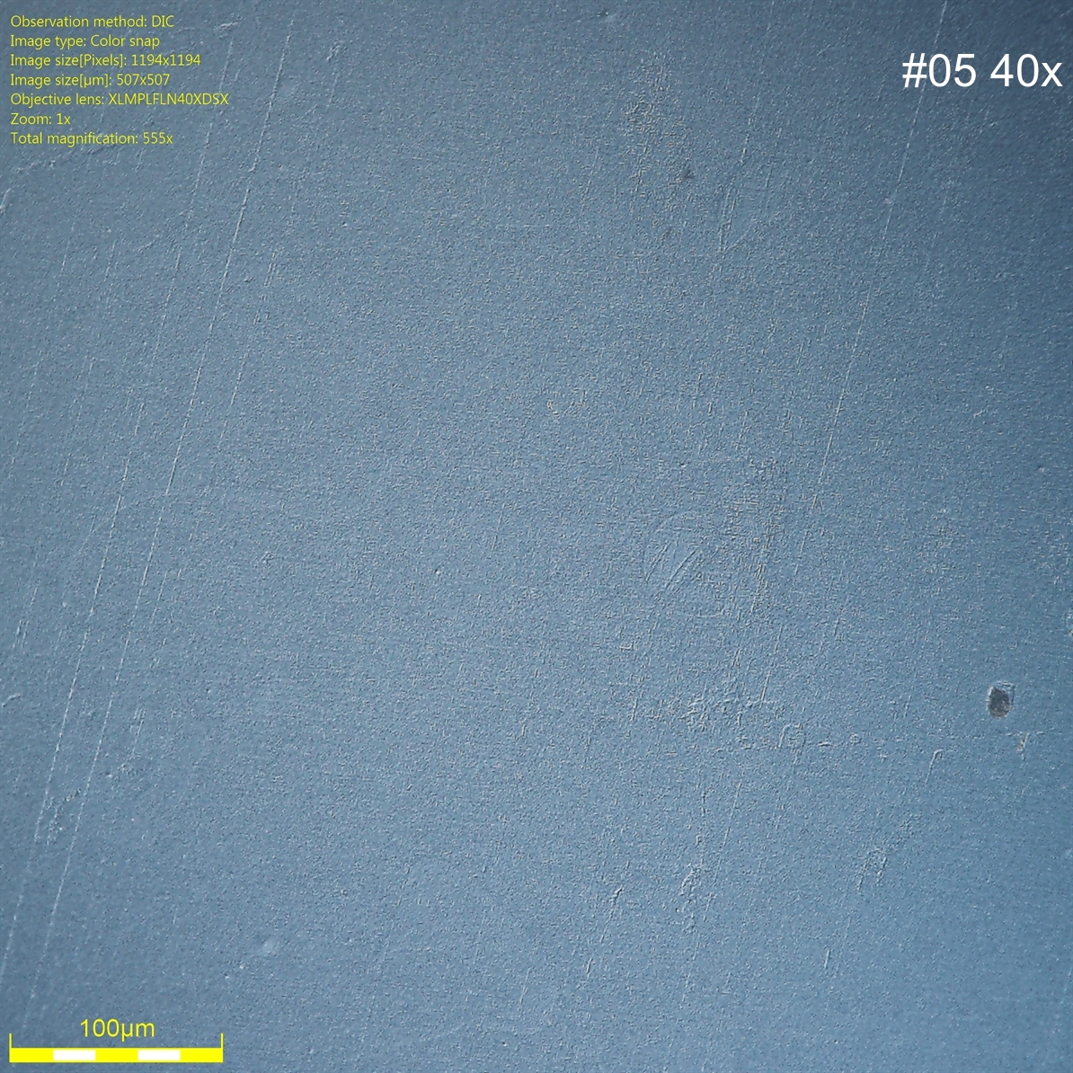
We do not look on dots, points and other small defects, as they are
cleaving dust or substrate preparation. We look on smoothness of
surface, Nomarsky contrast with HDR is extremely sensitive to rough
surface.
It could be seen, that FZU grown buffers on etched substrates have
smoother surface, not etched substrates give “higher grain texture”.
Next steps will be:
-
Etch GaSb substrate, and grow thicker buffer, to narrow down optimum growth conditions, and confirm with AFM
-
Test GaSb buffers on GaAs
-
Ternary AlGaSb, InGaSb, AsGaSb
-
Test buffers with TEGa + TESb
…